-

-

-

- HOME
- 연구동향
- MERRIC인
- 메릭웨비나
- 공학DB
- 문헌정보
- 기계로봇소식
- MERRIC은?
- 회원가입
- 로그인

- 물성치테이블
- 용어사전
- 실험실소개
| 지도교수 | 송종인 |
|---|---|
| 전공분류 | 기타(ETC), |
| 주소 | A-315 Department of Information and Communications, Gwangju Institute of Science and Technology, 1 Oryong-dong Buk-gu Gwangju 500-712 Korea. |
| 전화 | 062-970-2277 |
| 홈페이지 | https://speed.gist.ac.kr/english/portal.php |
.jpg)
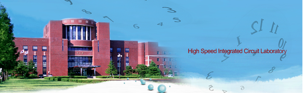
Primary research objectives of this laboratory include characterization of ultra-high-speed devices and circuits fabricated in the clean room, design of devices, integrated circuits, and subsystems for high speed optical and wireless communication system applications. The laboratory currently has a micro-wave probe station, a semiconductor parameter analyzer, two spectrum analyzers, a low-noise amplifier, a Silvaco device simulator, microwave circuit design simulators including HP Microwave Design Software (MDS),HP Advanced Desingn System(ADS) ,HSPICE, and work stations. The laboratory is using a vector network analyzer (VNA), microwave tuners, microwave power meters, microwave noise measurement system, and an HP ICCAP software for device parameter extraction now. These measurement system primary cover frequency ranges up to 50 GHz and we will upgrad to cover higher frequency ranges. Also we have a many measurement utilities related to Optics.On-going research projects in the laboratory are the development of millimeter-wave device and MMIC RF modules for 40 GHz LMDS system, the development of HBT power transistors for 30 GHZ LMDS system, and the development of opto-electrionic converter, photo diode(PD), laser diode(LD) and amplifier for millimeter-over-fiber (MMoF) sysetm, the development of InP-based HBT technology, and etc. Detailed research topics include epitaxial growth, device fabrication, device modelling and parameter extraction, microwave device (noise and power) characterization, MMIC design, MMIC fabrication, reliability of device and MMIC.
There is a clean room in the department, 4,320 square-feet-wide with the class of 1,000 to 10,000 depending on the specific area. The clean room is equipped with facilities for fabrication of compound semiconductor devices and circuits for high-speed communication applications. The fabrication equipments currently installed are a V80H chemical beam epitaxy system (CBE), molecular beam epitaxy (MBE), a J5800LV scanning electron microscope (SEM), a Raith Elphy Plus SEM-based e-beam lithography system, a Karl Suss Jirset Photoresist spin coater, a Karl Suss MJB3 mask aligner with a backside alignment capability, Leica optical microscopes, an Oxford Plus80 reactive ion etching (RIE) system, an Oxford Plus80 plasma enhance chemical vapor deposition (PECVD) system, a Temescal BJD-1800 e-beam evaporator system, an Alpha-step profiler, and chemical wet stations. The equipments are capable of fabricating ultra-high-speed devices including high-electron mobility transistors (HEMTs), heterojunction bipolar transistors (HBTs), high-speed detectors, and modulators operating up to a few hundred GHz and integrated circuits operating up to tens of GHz.
Generation and Transmission of a Quasi-Optical Single Sideband Signal for Radio-Over-Fiber Systems.
IEEE Photonics Technology Letters, 2011, Vol. 23, No. 6, pp. 0~ 0
Hyoung-Jun Kim, Jong-In Song
Full-Duplex WDM-based RoF System Using All-optical SSB Frequency Upconversion and Wavelength Re-use
IEEE Transactions on Microwave Theory and Techniques, 2010, Vol. 0, No. 0, pp. 0~ 0
김형준, 송종인
Photonic Frequency Upconversion Technique using an Electro-absorption Modulator for Radio-over-Fibre
Electronics letters, 2010, Vol. 46, No. 22, pp. 1~ 2
Phase noise characteristics of all-optical single sideband frequency upconverter for radio-over-fibr
Hyoung-Jun Kim, Jong-In Song
Electronics letters, 2010, Vol. 46, No. 10, pp. 1~ 2
Hyoung-Jun Kim, Ho-Jin Song, Jong-In Song
BER and SFDR Characteristics of an FWM-based All-Optical Frequency Upconverter.
Photonics Technology Letters, 2009, Vol. 0, No. 0, pp. 0~ 0
Hyoung-Jun Kim, Jong-In Song
All-optical single-sideband upconversion with an optical interleaver and a semiconductor optical amp
Optics express, 2009, Vol. 17, No. 12, pp. 0~ 0
Tae-Woo Kim, Dae-Hyun Kim, Sang-Duk Park, Seung Heon Shin, Seong June Jo, Ho-Jin Song, Young Min Par
A two-step recess process based on atomic-layer-etching.
IEEE Transaction on Electron Device, 2008, Vol. 55, No. 7, pp. 1577~ 1584
김태우, 김대현, 박상덕, 신승헌, 조성준, 송호진, 박영민, 배정운, 김영운, 염근영, 장재형, 송종인
A Two-Step-Recess Process Based on.
IEEE Trans. Electron Devices, 2008, Vol. 55, No. 7, pp. 1577~ 1584
Tae-Woo Kim, Dae-Hyun Kim, Sang Duk Park, Geun Young Yeom, Byeong Ok Lim, Jin-Koo Rhee, Jae-Hyung Ja
Effect of two-step recess process using atomic layer etching on performance of In0.52Al0.48As/In0.53
IEEE Electron Device Letters, 2007, Vol. 28, No. 12, pp. 1086~ 1088
Soo-Ghang Ihn, Mee-Yi Ryu, Jong-In Song
Optical properties of undoped, Be-doped, and Si-doped wurtzite-rich GaAs nanowires grown on Si subst
Solid State Communications, 2010, Vol. 0, No. 0, pp. 0~ 0